- 您现在的位置:买卖IC网 > Sheet目录2098 > MK2069-01GILFTR (IDT, Integrated Device Technology Inc)IC VCXO CLK SYNCHRONIZER 56TSSOP
MK2069-01
VCXO-BASED LINE CARD CLOCK SYNCHRONIZER
VCXO AND SYNTHESIZER
IDT VCXO-BASED LINE CARD CLOCK SYNCHRONIZER
3
MK2069-01
REV K 051310
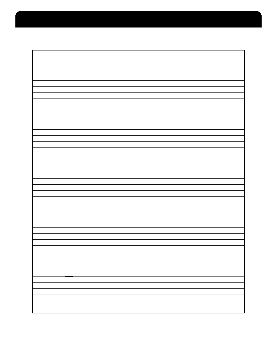
Pin Descriptions
Pin
Number
Pin
Name
Pin
Type
Pin Description
1
ST0
Input
Scaling Divider bit 0 input, Translator PLL (internal pull-up).
2
ST1
Input
Scaling Divider bit 1 input, Translator PLL (internal pull-up).
3
RT0
Input
Reference Divider bit 0 input, Translator PLL (internal pull-up).
4
RT1
Input
Reference Divider bit 1 input, Translator PLL (internal pull-up).
5
FT0
Input
Feedback Divider bit 0 input, Translator PLL (internal pull-up).
6
FT1
Input
Feedback Divider bit 1 input, Translator PLL (internal pull-up).
7
FT2
Input
Feedback Divider bit 2 input, Translator PLL (internal pull-up).
8
FT3
Input
Feedback Divider bit 3 input, Translator PLL (internal pull-up).
9
FT4
Input
Feedback Divider bit 4 input, Translator PLL (internal pull-up).
10
FT5
Input
Feedback Divider bit 5 input, Translator PLL (internal pull-up).
11
RV0
Input
Reference Divider bit 0 input, VCXO PLL (internal pull-up).
12
VDDT
Power
Power Supply connection for translator PLL.
13
GNDT
Ground
Ground connection for translator PLL.
14
X1
-
Crystal oscillator input. Connect this pin to the external reference crystal.
15
VDDV
Power
Power Supply connection for VCXO PLL.
16
X2
-
Crystal oscillator output. Connect this pin to the external reference crystal.
17
GNDV
Ground
Ground connection for VCXO PLL.
18
LFR
-
Loop filter connection, reference node. Refer to loop filter circuit on page 6.
19
LF
-
Loop filter connection, active node. Refer to loop filter circuit on page 6.
20
ISET
-
Charge pump current setting input. Refer to loop filter circuit on page 6.
21
FV0
Input
Feedback Divider bit 0 input, VCXO PLL (internal pull-up).
22
FV1
Input
Feedback Divider bit 1 input, VCXO PLL (internal pull-up).
23
FV2
Input
Feedback Divider bit 2 input, VCXO PLL (internal pull-up).
24
FV3
Input
Feedback Divider bit 3 input, VCXO PLL (internal pull-up).
25
FV4
Input
Feedback Divider bit 4 input, VCXO PLL (internal pull-up).
26
FV5
Input
Feedback Divider bit 5 input, VCXO PLL (internal pull-up).
27
FV6
Input
Feedback Divider bit 6 input, VCXO PLL (internal pull-up).
28
FV7
Input
Feedback Divider bit 7 input, VCXO PLL (internal pull-up).
29
FV8
Input
Feedback Divider bit 8 input, VCXO PLL (internal pull-up).
30
FV9
Input
Feedback Divider bit 9 input, VCXO PLL (internal pull-up).
31
FV10
Input
Feedback Divider bit 10 input, VCXO PLL (internal pull-up).
32
FV11
Input
Feedback Divider bit 11 input, VCXO PLL (internal pull-up).
33
MX1
Input
Input MUX selection bit 1 (internal pull-up).
34
ICLK2
Input
Reference clock input 2.
35
ICLK0
Input
Reference clock input 0. 5V tolerant input.
36
CLR
Input
Clear input, clears VCXO PLL dividers when low (internal pull-up).
37
LDC
-
Lock detector threshold setting circuit connection. Refer to circuit on page 10.
38
GND
Ground
Digital ground connection.
39
LDR
-
Lock detector threshold setting circuit connection. Refer to circuit on page 10.
40
RCLK
Output
VCXO PLL phase detector Reference Clock output.
41
GNDP
Ground
Ground connection for output drivers (VCLK, TCLK, RCLK, LD, LDR).
发布紧急采购,3分钟左右您将得到回复。
相关PDF资料
MK2069-04GILFTR
IC VCXO CLK TRANSLATOR 56-TSSOP
MK2302S-01LFTR
IC MULTIPLIER/ZD BUFFER 8-SOIC
MK2304S-2LF
IC PLL ZD BUFFER LO SKEW 8-SOIC
MK2703SILF
IC PLL AUD CLK SYNTHESIZER 8SOIC
MK2704SLF
IC PLL AUD CLK SYNTHESIZER 8SOIC
MK2716SLFTR
IC CLK SYNTHESIZER HDTV 8-SOIC
MK2732-06GLF
IC VCXO/MULTIPLIER 16-TSSOP
MK2745-21SLFTR
IC CLK SOURCE DVD/MPEG 16-SOIC
相关代理商/技术参数
MK2069-01GITR
功能描述:IC VCXO CLK SYNCHRONIZER 56TSSOP RoHS:否 类别:集成电路 (IC) >> 时钟/计时 - 时钟发生器,PLL,频率合成器 系列:- 标准包装:39 系列:- 类型:* PLL:带旁路 输入:时钟 输出:时钟 电路数:1 比率 - 输入:输出:1:10 差分 - 输入:输出:是/是 频率 - 最大:170MHz 除法器/乘法器:无/无 电源电压:2.375 V ~ 3.465 V 工作温度:0°C ~ 70°C 安装类型:* 封装/外壳:* 供应商设备封装:* 包装:*
MK2069-03
制造商:ICS 制造商全称:ICS 功能描述:VCXO-Based Clock Translator with High Multiplication
MK2069-03GI
功能描述:IC VCXO CLK TRANSLATOR 56-TSSOP RoHS:否 类别:集成电路 (IC) >> 时钟/计时 - 时钟发生器,PLL,频率合成器 系列:- 标准包装:27 系列:Precision Edge® 类型:频率合成器 PLL:是 输入:PECL,晶体 输出:PECL 电路数:1 比率 - 输入:输出:1:1 差分 - 输入:输出:无/是 频率 - 最大:800MHz 除法器/乘法器:是/无 电源电压:3.135 V ~ 5.25 V 工作温度:0°C ~ 85°C 安装类型:表面贴装 封装/外壳:28-SOIC(0.295",7.50mm 宽) 供应商设备封装:28-SOIC 包装:管件
MK2069-03GITR
功能描述:时钟发生器及支持产品 VCXO-BASED CLOCK TRANSLATOR RoHS:否 制造商:Silicon Labs 类型:Clock Generators 最大输入频率:14.318 MHz 最大输出频率:166 MHz 输出端数量:16 占空比 - 最大:55 % 工作电源电压:3.3 V 工作电源电流:1 mA 最大工作温度:+ 85 C 安装风格:SMD/SMT 封装 / 箱体:QFN-56
MK2069-04
制造商:ICS 制造商全称:ICS 功能描述:VCXO-Based Universal Clock Translator
MK2069-04GI
功能描述:IC VCXO CLK TRANSLATOR 56-TSSOP RoHS:否 类别:集成电路 (IC) >> 时钟/计时 - 时钟发生器,PLL,频率合成器 系列:- 标准包装:39 系列:- 类型:* PLL:带旁路 输入:时钟 输出:时钟 电路数:1 比率 - 输入:输出:1:10 差分 - 输入:输出:是/是 频率 - 最大:170MHz 除法器/乘法器:无/无 电源电压:2.375 V ~ 3.465 V 工作温度:0°C ~ 70°C 安装类型:* 封装/外壳:* 供应商设备封装:* 包装:*
MK2069-04GILF
功能描述:时钟发生器及支持产品 VCXO-BASED UNIVERSAL CLOCK TRANSLATOR RoHS:否 制造商:Silicon Labs 类型:Clock Generators 最大输入频率:14.318 MHz 最大输出频率:166 MHz 输出端数量:16 占空比 - 最大:55 % 工作电源电压:3.3 V 工作电源电流:1 mA 最大工作温度:+ 85 C 安装风格:SMD/SMT 封装 / 箱体:QFN-56
MK2069-04GILFTR
功能描述:时钟发生器及支持产品 VCXO-BASED UNIVERSAL CLOCK TRANSLATOR RoHS:否 制造商:Silicon Labs 类型:Clock Generators 最大输入频率:14.318 MHz 最大输出频率:166 MHz 输出端数量:16 占空比 - 最大:55 % 工作电源电压:3.3 V 工作电源电流:1 mA 最大工作温度:+ 85 C 安装风格:SMD/SMT 封装 / 箱体:QFN-56